
A first board can look perfect on a screen and still fail the second it reaches your bench. That is the hard lesson many hobbyists, students, and new hardware founders learn after paying for fabrication, waiting on shipping, and opening a package full of boards that almost work. Circuit Board Design is not only about connecting the right pins. It is about thinking through current paths, heat, assembly, noise, and the small physical details that software can hide from you. For Americans building garage prototypes, school projects, repair tools, or early product samples, the cost is not only the board order. It is the lost weekend, the missed demo, and the parts you now have to desolder by hand. Good electronics project planning starts before routing begins, because small layout choices decide whether the final board feels clean or fights you at every step. The encouraging part is simple: most beginner failures are predictable. You can avoid them once you know where they start.
Starting With a Schematic That Looks Finished but Thinks Poorly
A clean schematic can fool you. Neat symbols, straight wires, and tidy labels give the project a false sense of order, especially when the circuit came from a breadboard that already blinked an LED or powered a sensor. The trouble begins when that sketch becomes a manufactured object. Breadboards forgive long jumper wires. PCBs do not. The first phase is where beginner electronics projects often fail quietly, before a single trace is drawn.
Trusting Library Parts Without Checking the Real Component
Wrong footprints ruin boards in a way that feels unfair. The circuit is correct. The code works. The datasheet was open on your laptop. Then the USB-C connector arrives, and its pads do not match your board. That one mistake can turn an otherwise solid project into a coaster.
Library footprints are useful, but they are not promises. A 0603 resistor footprint may work across many brands, yet connectors, switches, relays, battery holders, and modules can vary enough to cause pain. Even a pin header can create trouble if the hole size fits one supplier’s part and not the one you ordered from Digi-Key, Mouser, Amazon, or a local electronics shop.
Print the layout at 1:1 scale before ordering. Place the real parts on the paper. This looks old-school, but it catches what zoomed-in software hides. For surface-mount ICs, compare the land pattern against the datasheet package drawing, not the product photo. A counterintuitive truth: the parts that look easiest, such as buttons and connectors, often cause more board spins than the tiny chips beginners fear.
Leaving Power Intent Out of the Drawing
Many first schematics show power as a name, not a path. A net label says 5V or 3V3, so the designer assumes the job is done. Yet power needs source capacity, return path, local storage, and protection. A board that ignores these details may boot once, reset when a motor starts, or behave differently when powered from USB instead of a bench supply.
Beginner electronics projects often mix modules, sensors, displays, and microcontrollers from different tutorials. Each part may work alone. Together, they can pull more current than expected or inject noise into a shared rail. A small OLED, a Wi-Fi module, and a relay coil can expose weak power planning fast.
Add test points for main rails. Mark expected voltage near them. Place bulk capacitance near power entry and small decoupling capacitors near IC pins. KiCad’s official documentation also describes design-rule checks that can catch missing connections, clearance issues, and minimum-width violations, which helps only after you define rules that match the board you plan to build.
The non-obvious part is that power planning is not only for high-current boards. A low-power sensor board can fail from poor return paths and weak decoupling long before it fails from lack of current.
The Hidden Setup Errors Behind Circuit Board Design
Once the schematic feels ready, beginners often rush into placement and routing. That rush creates the next layer of mistakes. The board editor opens with default rules, default grid settings, and default assumptions. Those defaults may be fine for a practice board, but they may not match the factory, the parts, or the way the circuit will be assembled. This is where the design starts becoming physical.
Ignoring Manufacturer Rules Until the End
Fabricators publish limits for trace width, copper spacing, drill size, annular ring, solder mask clearance, board outline, and slot handling. Beginners often treat those as paperwork. Then the board fails review, or worse, passes review but comes back fragile.
A two-layer Arduino-style shield with big through-hole parts may tolerate relaxed choices. A small sensor board with USB, QFN parts, and tight connectors does not. If your selected manufacturer allows 6 mil traces but charges less for 8 mil traces, that choice matters. Wider rules can make the board cheaper, easier to inspect, and less likely to contain ugly compromises.
Set the board rules before placement. Do not route first and hope the design-rule checker will clean up later. That approach creates a maze of near-misses. It also trains bad habits, because you start solving electrical problems with geometry instead of planning. Good PCB routing tips begin with restraint: choose rules you can build, solder, and inspect, not the smallest values the factory will accept.
Use your manufacturer’s published capabilities as the board setup baseline. Then run DRC early and often. The checker is not a judge at the finish line. Treat it like a smoke alarm.
Designing for the Screen Instead of the Workbench
A PCB editor lets you zoom until a cramped layout looks roomy. Your hand does not have that luxury. Tweezers need space. A soldering iron needs angle. A multimeter probe needs a place to land. When beginners forget the workbench, PCB layout errors become human errors.
Think about a small ESP32 project board. If the reset button sits between a tall electrolytic capacitor and a USB connector, it may be hard to press once the board is installed in a plastic case. If test pads sit under a display module, they are test pads in name only. If the silkscreen labels face the wrong direction, every repair becomes slower.
A board should explain itself after assembly. Label power input, polarity, programming pins, sensor ports, and jumper settings. Place pin 1 marks where they can still be seen after the part is installed. Keep connectors aligned with how wires will leave the enclosure, not with what makes routing look pretty.
Here is the odd lesson: a slightly larger board may be the more professional board. Beginners often shrink layouts to prove skill. Experienced designers leave room where touch, heat, wiring, and inspection demand it.
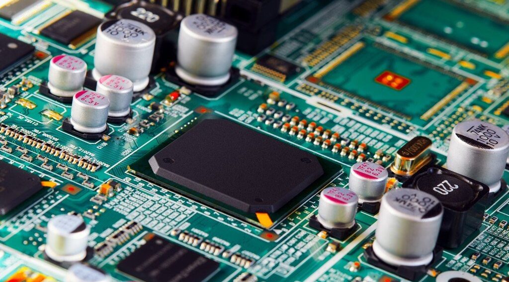
Routing Mistakes That Turn Good Circuits Into Bad Boards
Routing feels like the main event, so beginners spend hours making traces look clean. Clean is good. Electrical sense is better. A neat board can still suffer from noise, weak current paths, poor grounding, and signals that interfere with each other. The trace is not a line on a drawing. It is part of the circuit.
Treating Ground Like Another Signal Trace
Ground is not a trash net where all returns disappear. Current leaves a source and comes back through a return path. When that path is chopped up, forced through thin necks, or split by random traces, the board can become noisy and unpredictable.
On a simple two-layer board, a mostly solid ground plane on one layer is often the safest habit. Route signals and power with care, then keep the return path short and direct. Do not slice the ground plane into islands unless you know why. A broken plane under a clock line, USB pair, or sensor signal can cause more trouble than the trace itself.
A real example: a beginner builds a small audio preamp board and routes ground as a thin daisy chain from jack to op-amp to power input. It passes continuity. It may even make sound. Then it hums when touched or when placed near a laptop charger. The schematic did not show that loop area. The layout created it.
The quiet insight is that ground mistakes often look like software bugs. A microcontroller reset, ADC jitter, or sensor spike may send you into code for hours, while the board is begging for a better return path.
Making Traces Too Thin, Too Close, or Too Casual
Trace width is not decoration. It affects resistance, heat, voltage drop, and manufacturability. Trace spacing affects noise, arcing risk, solder bridges, and whether the fabricator can make the board without drama. Some beginner PCB layout errors come from treating all nets the same.
Power traces need more copper than logic traces. Motor, LED strip, relay, heater, and battery paths need special attention. If a trace carries current that would warm a jumper wire, do not route it like a signal line. Use wider copper, pours, short paths, and connector placement that does not force current through a skinny corner.
Spacing deserves the same respect. Keep noisy nets away from sensitive ones. Do not run a switching regulator node beside an analog sensor trace because it saves space. Do not place crystal traces long and wandering across the board. Keep related parts close, and give signals room when the board allows it.
Good PCB routing tips are not about making every board look like a high-speed motherboard. They are about matching the route to the job. A slow button signal can be relaxed. A USB signal, clock, RF feed, or high-current load cannot be treated as casual copper.
Assembly, Testing, and Handoff Mistakes That Cost the Most
The final group of mistakes hurts because it appears late. The board arrives. The solder paste is ordered. The parts are on the desk. Then you notice the connector faces inward, the programming header is missing, or the assembly house has questions your files do not answer. This stage separates a board that can be built once from a board that can be built again.
Forgetting How the Board Will Be Soldered
A design can be electrically correct and still painful to assemble. Beginners often place tall parts too close to small surface-mount parts, crowd polarized components, or mix packages in a way that makes hand soldering harder than it needs to be.
If you plan to solder by hand, choose parts your tools can handle. There is no shame in using 0805 passives instead of 0402 parts on a first board. A slightly larger resistor can save hours of frustration. For a school robotics controller or home weather station, serviceability beats density.
Think about assembly order. Tall connectors, terminal blocks, relays, and large capacitors may block access to nearby pads. Heat-sensitive parts should not sit where repeated rework will punish them. Place polarized components with consistent orientation where possible. Diodes, LEDs, electrolytic capacitors, IC pin 1 marks, and connector labels should be easy to read.
This is where PCB soldering basics can matter as much as routing skill. A beginner who designs for the soldering process gets better results with ordinary tools. A beginner who designs only for the software view may need expensive gear to recover from small choices.
Skipping Test Points and Revision Clues
No first board should assume success. Add test points. Add labels. Add a revision mark. Add mounting holes if the board will live inside anything. These choices seem boring until the board fails and you need answers fast.
Test points should cover power rails, reset, programming lines, key sensor signals, and ground. They do not need to be fancy. A small exposed pad can save the day. Put ground test points near areas where you will probe. A single ground clip location at the far edge of the board can make debugging harder than needed.
Revision labels matter too. Mark the board as Rev A, Rev 1, or with a date code. When three versions sit on your bench, you will not remember which one fixed the regulator pinout. Students, makers, and small U.S. startups often learn this after mixing prototype batches in the same storage bin.
Before exporting Gerbers, make a short release checklist. Confirm footprints, polarity, mounting, board outline, drill files, solder mask, silkscreen, and DRC status. Save that checklist with the project. A simple electronics tool checklist can also keep parts, probes, flux, wire, and adapters from becoming last-minute obstacles.
Conclusion
Your first board does not need to be perfect. It needs to teach the right lessons without punishing you for every small miss. The best beginners slow down before fabrication, check the physical world against the screen, and design for debugging before they need it. Circuit Board Design rewards that kind of patience. It is less about drawing clever traces and more about respecting how electricity, copper, solder, parts, and hands meet on one small surface. A board that is easy to inspect, power, probe, and repair will usually beat a tiny layout that looks impressive in a screenshot. Start with wider margins. Choose parts you can solder. Keep ground honest. Run checks before the final hour. Then order the board with confidence, not crossed fingers. Your next project will be cleaner because this one was built to be understood.
Frequently Asked Questions
What is the most common PCB mistake beginners make?
Wrong footprints are among the most damaging beginner mistakes because the circuit can be correct while the parts still do not fit. Always compare the footprint against the datasheet package drawing and print the board at actual size before ordering.
How do I avoid bad PCB layout errors in my first project?
Start with manufacturer rules, place parts by function, keep power paths short, and preserve a clean ground return. Run DRC early instead of waiting until export. Most layout trouble grows from rushed setup and poor placement.
Is a two-layer PCB enough for beginner electronics projects?
Yes, many first boards work well on two layers when the circuit is modest. Use one layer mainly as ground where possible, keep routing simple, and avoid mixing high-current loads with sensitive analog signals unless you plan the paths carefully.
Why does my PCB work on a breadboard but fail after fabrication?
A breadboard hides layout issues such as return paths, decoupling distance, connector orientation, and power noise. The PCB turns those choices into copper. A circuit that works with jumpers can fail when layout choices add resistance, noise, or bad access.
How close should decoupling capacitors be to IC pins?
Place small decoupling capacitors close to the IC power pins with short paths to power and ground. The goal is to supply fast local current and reduce noise. Long traces weaken the capacitor’s effect, even when the schematic looks correct.
What PCB routing tips matter most for a first board?
Keep related parts close, make power traces wide enough, avoid broken ground paths, and separate noisy signals from sensitive ones. Do not chase a beautiful route at the cost of electrical sense. A plain, readable board often performs better.
Should beginners use smaller SMD parts to save board space?
Use parts you can assemble with your tools. For hand soldering, 0805 or 0603 passives are often friendlier than tiny packages. Saving a few millimeters is not worth a board that becomes hard to solder, inspect, or repair.
Do I need test points on a simple PCB?
Yes, even simple boards benefit from test points. Add them for power rails, ground, reset, programming pins, and key signals. They make debugging faster and prevent you from scraping solder mask or holding probes on tiny IC pins.